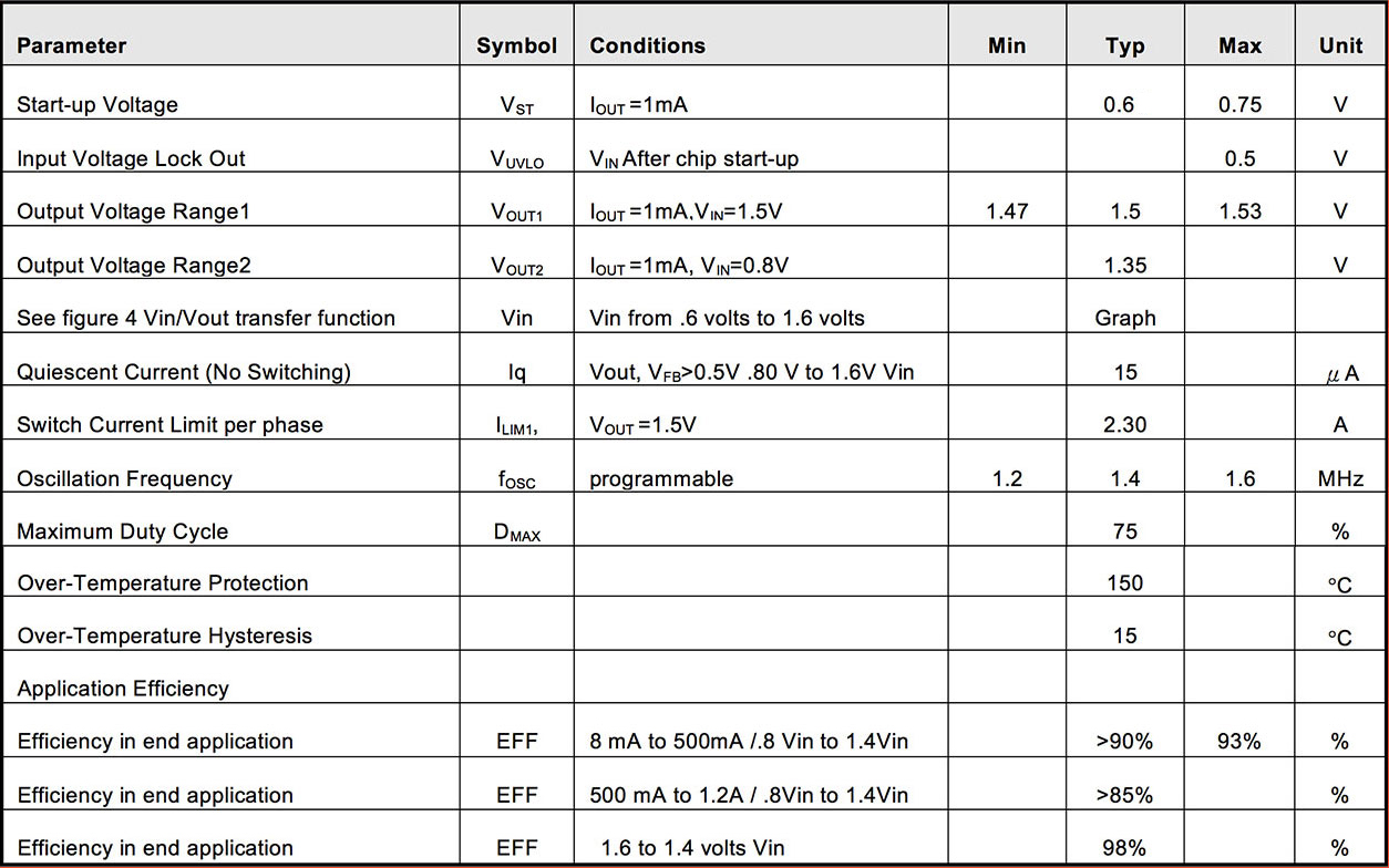
The BTR004 is a high efficiency, fixed interleaved frequency 1.4MHz, current mode PWM boost DC/DC converter which could operate from single-cell NiCd, NiMH or alkaline battery such as input voltage below 0.6V. The converter output voltage is adjusted from 1.5V to 1.32V from VIN at 1.5V to 0.80V. No external Schottky diode is required and the converter can achieve efficiency of 93%.
The converter is based on a fixed frequency, current mode, pulse-width-modulation PWM controller that goes automatically into burst mode at light load which quiescent current is only 15uA in this mode of operation. When converter operates in discontinuous mode, the internal anti-ringing switch could reduce interference and radiated electromagnetic energy. The BTR004 is available in a space-saving 8-lead DFN package for portable application
Read More...
Features
Synchronous Rectification: 93% Efficiency
Very Low Start-up Voltage at 0.6V
Automatically Switch to Burst Mode for Improving Efficiency at Light Load
Internal Anti-Ringing Switch across Inductor
Fixed Interleaved Frequency Operation at 1.4MHz with 2.8Mhz clock
Small 8-Pin DFN Package
RoHS Compliant
Increases battery life up to 600%.
Applications
Single-cell NiCd, NiMH or alkaline battery
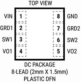
PIN ASSIGNMENTS
Figure 1. Pin Assignment of BTR004
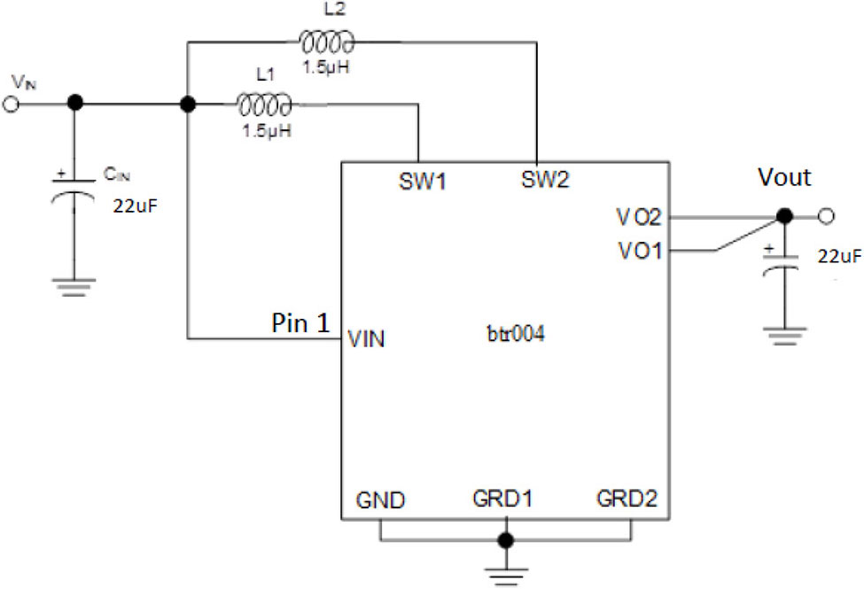
BOARD LAYOUT
Figure 2- Typical Circuit
PRELIMINARY
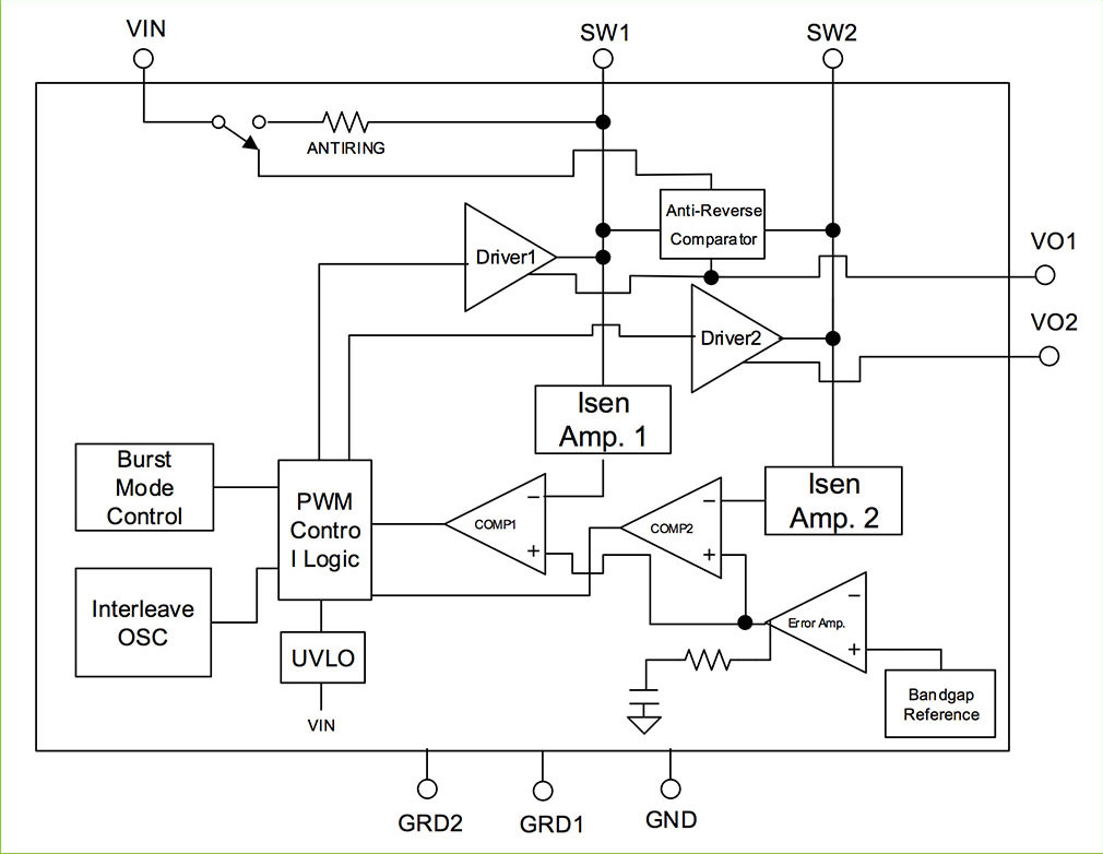
Figure 3- Block Diagram of BTR004
Absolute Maximum Ratings
Supply Input Voltage (VIN ,VOUT,FB) ----------------- -0.3 to + 1.8V
SW Voltage(VSW1,VSW2)-------------------------------- -0.3 to +1.8V
Storage Temperature Range(TS)--------------------- -65 to + 150℃
Lead Temperature (Soldering, 10 sec.)(TLEAD)-----------+ 260℃
Note 1:Stresses greater than those listed under "Absolute Maximum Ratings" may cause permanent damage to the device. These are stress ratings only and functional operation of the device at these or any other conditions beyond those indicated under “Recommended Operating Conditions” are not implied. Exposure to "Absolute Maximum Ratings" for extended periods may affect device reliability.
Recommended Operating Conditions
Input Voltage(VIN)------------------------------------------------+ 0.5 to VOUT
Typical Performance Curves of Battery Life Extender with IC
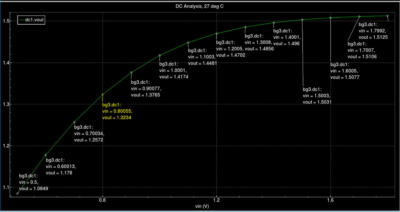
The Vin/Vout transfer function of the IC optimizes alkaline batteries' performance in the many applications world wide. Alkaline batteries operate from 0.8 volts to 1.6 volts where a new battery is typically ~1.6 volts and all the energy is depleted by the time the battery voltage reaches the 0.8 volt level. In order to optimize the batteries energy consumption from 1.6 volts to .80 volts, this transfer function enables good operation of the applications until the battery has been fully depleted energy at the .80 volt energy level. The application will still be operating at 1.32 volts at the terminals of the “Batteroo Life Extender” when the battery voltage is dropped to 0.80 volts. This programmable transfer function can be adjusted to optimize for different requirements. The key result is that most of applications will have the battery energy depleted and will have solid application performance as the battery energy is consumed causing the voltage level of the battery to reach 0.80 volts. A typical battery will cause the end applications to not perform well and/or shutdown as it reaches the 1.1 to 1.3 volts cut off voltage of the battery operated device. Even when the cut off voltage of the device is around 1.1v, Devices stop operating at the higher voltage levels. This is due typically to higher transient currents (causing significant voltage drop inside the battery due to internal resistance of the battery) than just the steady state current draw of the application. The end result is that the battery is thrown away with a lot of energy still left in its chemical technology. With the Patent Pending Batteroo Boost technology, the application will work until the battery voltage reaches 0.80 volts. This causes the battery operated devices to use the energy that would have been thrown away and be able to have a longer operating life for the device; in turn extending the useful life of the battery in that device.
Read More...
Figure 4- Vin/Vout transfer function
Functional Description
The circuit is a high efficiency, fixed interleaved frequency 1.4MHz, current mode PWM boost DC/DC converter. It consists of an Input Pin in which the battery input voltage is applied to the IC. There are two phases in the circuit in which 2 inductors are attached to the Vin and the two switch nodes of SW1 and SW2 respectively. At each node of the SW1 and SW2, there is a NFET1 and a NFET2 that connects to ground from the respective inductor. There is also PFET1 and PFET2 that are attached from SW1 and SW2 to the output voltage pins. The output voltage pins VO1 and VO2 are connected together to form one output for the application. Overall you have two boost circuits interleaved at 180 degrees with each one providing half of the power to the output. The NFET turns on at a duty cycle determined by the EA monitoring the output voltage. Once the NFET completes its Ton times, it turns off and the PFET turns on for the remainder of the cycle thus giving the circuit a synchronous switching between the NFET and the PFET with very fast rise times to minimize switching losses.
The circuit operates at an internally trimmed clock of 1.4Mhz. Each phase operates at 180 degrees from each other. Each phases Ton is set by the same EA signal so that the current ramp signal is sensed by the comparator1 and comparator2 and both of these signals are compared to the common EA signal so that both currents during the NFET on time are matched against a common EA signal and logic. This insures current sharing between the two phases but does not account for the difference of current amplitude caused by the tolerance of inductance in the circuit which is minimal. The circuit also runs in burst mode once you are below a predetermined current level for improved efficiency at lighter load conditions.
The EA is internally compensated by a Pole and a Zero in order to shape the phase gain response of the Boost converters small signal transfer function. The circuit is very stable under all conditions. The VO1 and V02 are compared against a reference which is further modified by a set of trimmed resistors internal to the circuit. This signal is fed into the EA and is modified by the Pole and Zero properties in the transfer function to give an output in which both current signals are independently compared to for a good current mode control. Internally there is slope compensation on the current sense signals to insure that once you go past a perdetermined point in the duty cycle, the circuit will not exhibit any subharmonic oscillations and the circuit remains stable throughout the entire frequency domain.
The circuit has internal temperature shutdown where the NFET temperature is monitored. An OVP signal independently operates to shut down the circuit if an overvoltage condition occurs..
Read More...
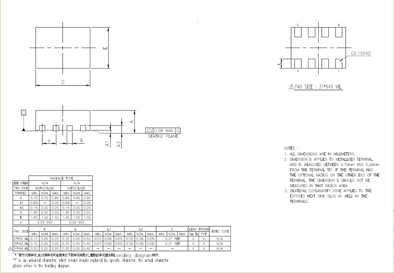
Board Layout Thermal Information- 150C shutdown
DFN-8 2x1.5 Package (Unit: mm)
Life Support Policy
BTR’s products are not authorized for use as critical components in life support devices or other medical systems.